It is reported that a few days ago, scientists successfully developed a 0.7nm tungsten selenide diode, which means that humans have finally broken the semiconductor 3nm process limit, and toward the development of semiconductor technology, and took a small step forward! Why do you say that? As you may be keen on semiconductors, semiconductor process technology is rapidly evolving with the development of smartphones from 28nm, 16nm, 10nm, 7nm, 5nm to 3nm. However, in this process, the miniaturization process of the semiconductor process is also slowing down due to the gradual failure of Moore's Law.
What is Moore's Law? This was proposed by Gordon Moore, one of Intel's founders, in 1965. When the price is constant, the number of components that can be accommodated in a semiconductor chip will double in about two years, and its performance will increase year-on-year.
chip for cell phone picture
Why is the price unchanged? This is beyond doubt. Because, from the perspective of the public, it is natural to buy a mobile phone with a relatively high cost performance. If the price of semiconductors rises geometrically due to process factors, the price of mobile phones naturally rises. Of course, this situation does not exist because its promotion and application are not practical.
In addition, the industry generally believes that semiconductor manufacturing processes of 7nm or less are more difficult. For example, wafer etching is more difficult, and physical effects such as heat, electrostatic discharge, and electromagnetic interference are more significant... The point is, 7nm or even more The design and development costs of small processes are very high. From this point of view, it is no wonder that many people think that Moore's Law is coming to an end.
semiconductor picture
Therefore, the 0.7nm developed by the Taiwan University team, that is, a tungsten di-selenide diode (a two-dimensional single-atom diode) with only a single atomic layer thickness, is considered to be expected to surpass Moore's Law. In addition, according to the research team leader, WSe2 diodes are not only thinner, but also more efficient. In addition to the industry value of component cost/energy/speed optimization, they can also meet future artificial intelligence chips and machine learning. The need for a large amount of computational power.
So, what exactly is this tungsten selenide (WSe2)? This two tungsten selenide, as big as the graphene, is a two-dimensional nanomaterial with many unique physical and chemical properties, which is considered to be a revolutionary impact for many fields such as computers and communications. presence.
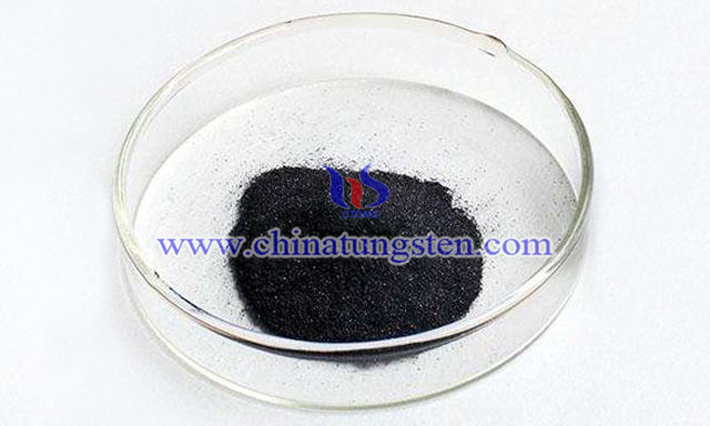
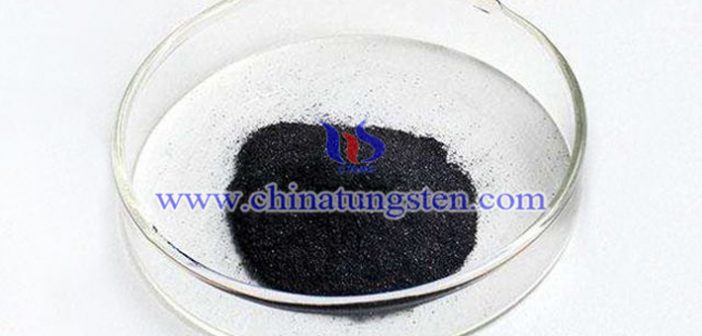
WSe2 picture
To a small point, tungsten selenide is a transition metal disulfide compound (TMDs) that exhibits excellent semiconductor transmission characteristics in the thickness of a single atomic layer (about 0.7 nm) compared to conventional silicon semiconductors. The material, in terms of thickness, has exceeded the process limit of 3 nm; in application, it can fully meet the requirements of the next generation of integrated circuits - thinner, smaller, faster.
Of course, scientists are also interested in other two-dimensional nanomaterials with unique physical and chemical properties and great application value, such as tungsten trioxide, molybdenum trioxide, titanium dioxide, zinc oxide, etc. in transition metal oxides. interest. In fact, so far, human research on two-dimensional nanomaterials is not particularly deep. I hope that our researchers, our little pride, will continue to work hard to develop new two-dimensional nanomaterials and unearth their huge potential. value. It is believed that in the near future, two-dimensional nanomaterials will be widely used not only in semiconductors, but also in many fields such as catalysis, energy storage, sensors, and solar cells.

