It is reported that graphene is gradually becoming a hot spot in the global scientific and technological community. According to experts, in addition to graphene, this two-dimensional material is gradually entering the field of science and technology.
In other words, what are the most popular words in your mind since the 21st century? Is there a place for 3D/3D? Although it is strange to separate them from specific applications, if you talk about 3D movies and 3D printing, you should not be unfamiliar. As we all know, in these areas, 3D means better visual effects, but also means higher technical level. However, for some areas, things are not like this, for example, two-dimensional materials.
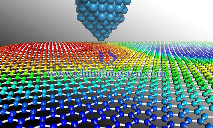
grapheme picture
Among the two-dimensional materials, everyone is more familiar with graphene. In 2004, the Geim team at the University of Manchester in the United Kingdom successfully separated the monoatomic graphite material, which is graphene. Since then, the concept of two-dimensional materials has been born and has spread throughout the scientific community. In this way, two-dimensional materials composed of atoms have successfully entered the stage of history.
As you may know, two-dimensional semiconductor materials have superior physical and optoelectronic properties, such as high light transmittance, high stability, and direct bandgap structure. Therefore, in the past scientific community, two-dimensional materials have attracted wide attention and have potential technical application prospects in many fields. Among them, graphene, as a two-dimensional semiconductor material, is widely used in the manufacture of photodetectors.
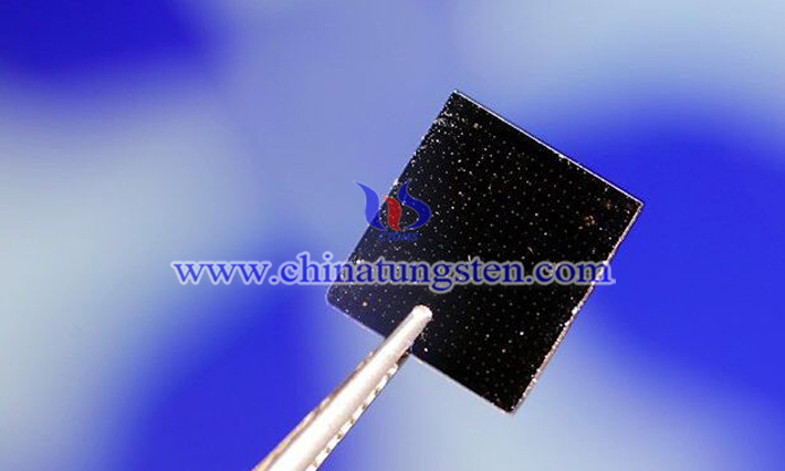
grapheme photoelectric detector picture
However, graphene photodetectors have certain limitations, such as low response rate, slower photo response time, and low external quantum efficiency (0.1-0.2%). Therefore, in order to find other photodetector two-dimensional materials to improve the response rate and spectral selectivity, scientists' enthusiasm for graphene has gradually expanded to other two-dimensional materials, and therefore, more and more two-dimensional materials. Was discovered and studied. Two-dimensional nanomaterials mainly include transition metal sulfides, transition metal oxides, and boron nitride.
At this point, we must first understand what is a photodetector? Photodetectors refer to materials that are subject to changes in the conductivity of the material itself. That is to say, the photodetector can convert the optical signal into an electrical signal. Therefore, photodetectors have a wide range of applications in civil, industrial, scientific, military and other fields, such as infrared remote sensing, missile guidance, infrared thermal imaging, industrial automation, radiometry and detection, photometric measurement and other fields.
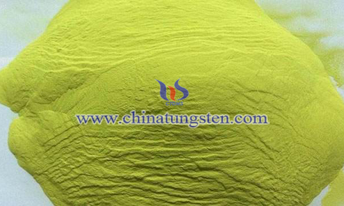
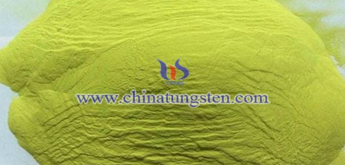
tungsten trioxide picture
In other words, in recent years, transition metal sulfide semiconductors (TMDCs) such as tungsten diselenide, molybdenum diselenide, and molybdenum disulfide have attracted great interest from researchers. Among all transition metal oxides, tungsten trioxide (WO3) is a wide bandgap n-type semiconductor material widely used in solar absorption, photochromism, military stealth and fuel cells. In recent years, tungsten trioxide dingal materials have attracted much attention with the rapid development of semiconductor research.
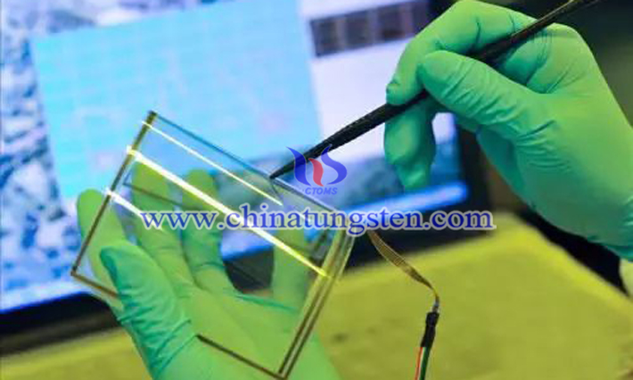
two dimensional WO3 nano film picture
The two-dimensional material that the experts mentioned at the beginning of the article is WO3 material. At present, the domestic research on tungsten trioxide mainly focuses on the preparation and doping of powder or film. The doped nano tungsten trioxide material has attracted more and more attention because of its special structure and properties. However, at present, there are few reports on two-dimensional tungsten trioxide nano-film photodetectors. Experts have found that from the few reports, the performance of WO3 photodetector components has many problems such as slow response time and low switching ratio. Therefore, experts set out to find new methods and ideas for film preparation and device fabrication to further improve the performance of WO3 photodetectors.
semiconductor picture
For example, some experts have used conventional chemical vapor deposition to synthesize two-dimensional WO3 nano-films of yttrium quality. Reports show that two-dimensional WO3 nano-films are connected with Cr/Au electrodes to produce a high-performance UV photodetector with excellent stability, reversibility, high on-off rate, fast response speed, and high sensitivity. And high external quantum efficiency. Experts say these features provide many new ideas and ideas for the fabrication and design of versatile and high-performance photodetectors based on layered semiconductor materials.

